How to make a Computer Inside a Computer with Julia

Computers have the remarkable property that they are capable of simulating a wide range of other systems, including themselves! But just because they can simulate themselves doesn't mean they should. No computer is 100% efficient, and so the computer being simulated must be slower than the computer simulating it. So why simulate a computer at all? It's actually fairly common practice to deploy applications on something called a virtual machine. A virtual machine is simply a computer being simulated inside another computer. The reason behind this is because some software is only compatable with certain computers. Some systems cannot run certain software out-of-the-box, but by simulating a computer that can run the software, any computer can run that software. Make sense? If not, that's ok, because we aren't going to be building a computer today so we can run legacy software on it, or deploy our applications on it. Rather, we will be building an extremely simple computer so that we can better understand how and why they work on a fundamental level.
In this article I will be talking about how to build an 8-bit computer using Julia code. But once again, why? Firstly, I think it will be fun and interesting. But more importantly, it will make building my 8-bit computer in Minecraft much simpler. We will be able to design and program our 8-bit computer in a much less restricted environment than Minecraft. Even if you don't plan on following the 8-bit Minecraft computer series I'm doing, building a computer with code still provides an opportunity to learn about how computers actually do execute programs.
Design
One of the beautiful things about computers in my opinion is that they are a collection of many different units which each do something rather unextraodinary, but when properly paired together, they can run programs and do calculations.
The Bus
In a computer, the bus is what all information flows across. It provides the mechanism for data from one part to reach another part, and connects everything together. Computers store information in binary, which is made up of two different states, usually denoted with either a 0 or a 1. This is because a standard wire can occupy 2 different states at once: whether the charge is positive or negative. Obviously we don't have to worry about currents and electric charge in our computer, but we still will have to represent the information on our bus. In our simulation, the bus will be able to carry 8-bits of information, hence our computer is an 8-bit computer.
Registers
A register stores a number. This number is the size of the bus, so in our case each register will store an 8-bit number. Each register is connected to the bus such that it can read in the value from the bus and store it, or write its stored value to the bus so that another component can access its value. In our computer, we will have 4 different registers. The first two are the A and the B registers. These have the special function as serving as inputs to the Arithmetic Logic Unit. The other two will be introduced later.
Arithmetic Logic Unit
This piece of the computer does math. In our computer, it will be able to perform either addition or subtraction, since the other operations can be implemented programatically using these two operations repeatedly. In an addition or subtraction problem, there are two inputs and one output. The two inputs will be fed into the ALU from the A register and the B register. The output of the ALU will also be attached to the bus so that the value can be moved to other parts of the computer. For example, we could feed the result of the addition operation back into the A register, and store a 1 in the B register, and we would have a circuit which counts up by repeatedly adding 1 to a number.
Random Access Memory
The Random Access Memory (more commonly referred to as RAM) is like the registers in that it can store numbers, but it can store far more than 1. In our computer it will only be able to store 16 different numbers for reasons I will discuss later. The way this is accomplished is by giving each of the numbers it stores a different address, similar to the street address given to a building. The third register in our computer is the Memory Address Register (MAR for short). This register will tell the RAM which address to read or write a number to or from the bus. The Random Access Memory is what will store our programs. Each consecutive line of our program will be placed in consecutive memory addresses inside our RAM.
Program Counter
We need some way of knowing which line of code (or memory address) our computer is currently executing. The program counter will be able to read a value from the bus, write its value to a bus (much like a register), and perform the additional function of counting up by 1. This way, we can initialize the Program Counter with a 0, and add 1 each time we finish executing a line of code.
Instruction Register
This is our fourth and final register. This register will store the current line of code we are executing. We can't simply execute our code directly from RAM because our code might modify the contents of our RAM. As such, we must store the current line of code inside the instruction register. Unlike other registers though, this register can only output 4 of its 8 bits that it stores.
Instruction Decoder
The instruction decoder is attached directly to the instruction register. Each instruction is made up of two 4-bit parts. The first 4-bit part is the operation. I like to think of the instruction as simply a statement telling the computer what to do. For example, we will define the instruction LDA later on, which takes a value from RAM and stores it in the A register. Since the instruction part of a line of code is 4 bits, we can have up to 16 different instructions that our computer can execute. The second half of the 8 bit instruction is called the operand. This tells our computer more detail on what to actually perform the operation on. For example, the operand of the LDA operation tells the computer what address in RAM to store in the A register. This is why our RAM will only be able to store 16 different numbers or lines of code: because our addresses can only be 4 bits long. There are ways around this limitation, but for the sake of simplicity I will not be addressing this limitation. If you forsee the small RAM size as a potential problem, feel free to expand my computer architecture to a larger bus size. A 16 bit computer of similar design could have 512 bytes of RAM (2 bytes per number, 256 numbers).
Design Diagram
That was a lot, and it can be difficult to see how all these pieces will fit together to make a computer. Below is a diagram of all these parts fitting together to form a functional computer architecture.
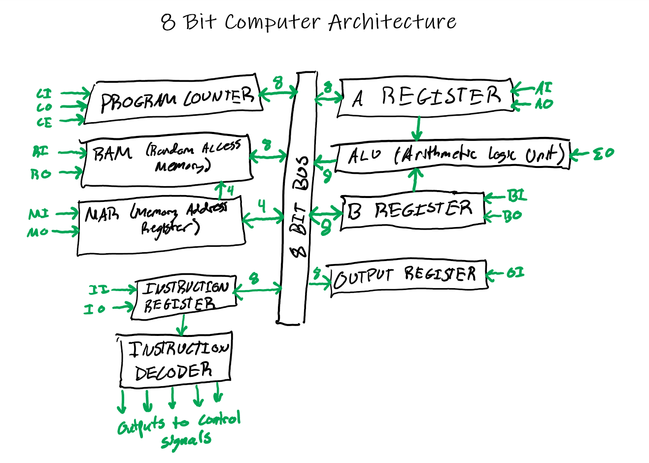
There's quite a bit going on in this diagram, but the biggest takeaway is that all these discrete components we spoke about in the previous section are connected to the bus in mostly the same ways, and that the instruction decoder is what actually manages the control signals for each of these components. A control signal is simply a signal which tells a component what action to perform. Remember how a register can either input or output a value from the bus? For example if we want to input to the A register we would turn on the AI control signal (stands for A register in). If we wanted to output the A register we would turn on the control signal AO. Every control signal is some sort of variant of an input or output of a certain component except one, the CE control signal. This can be found in the upper left corner connected to the program counter. We can input or output to the bus with CI or CO, but the CE control signal stands for "counter enable". All this means is that when the CE signal is on the program counter will increment the value it contains by 1.
At this point we know what each of the components should do, so now all that's left is to implement it in some Julia code!
Implementation
Before we get started, know that all the code for this project can be found at https://github.com/ctrekker/8-bit-vm.
Components
Firstly we want to define structures for each of our different components. This way we can build up our architecture in a more abstract way, only needing to connect the different components on a higher level.
The different components we need to implement are the bus, the register, the program counter, the ALU, and the RAM. Each of our components can be defined as instances of these components with the exception of the instruction decoder, which we will implement on a per-architecture basis due to its dependence on the makeup of the components.
Let's take a look at the simplest component: the bus
mutable struct Bus
    contents::UInt8
end
value(c::Bus) = c.contents
set_value(c::Bus, v::UInt8) = c.contents = v
Notice that the structure only contains one UInt8 type, which is a type of 8 bits in length. The value and set_value methods will be defined on every component. They will make it far easier to write abstract code where when we connect a component it doesn't matter what that component is so long as it is capable of having a value.
The bus is a little different in that it is not connected to the bus. For every other component we will subtype our structures under the abstract type Component we define below:
abstract type Component endNext we have the registers to implement. These need to store a value and be capable of outputting that value to a bus.
mutable struct Register <: Component
    value::UInt8
    bus::Bus
end
value(c::Register) = c.value
set_value(c::Register, v::UInt8) = c.value = v
Similarly to the bus, the register has a value that can be stored and retrieved, but it also stores a reference to a bus. Each component we implement from here on out will have a bus variable to store its connection to a bus.
The program counter is similar once again to the register, but has the added method enable, which will increment its current value by 1
mutable struct ProgramCounter <: Component
    value::UInt8
    bus::Bus
end
value(c::ProgramCounter) = c.value
set_value(c::ProgramCounter, v::UInt8) = c.value = v
enable(c::ProgramCounter) = c.value += 1
Next up is the ALU. This component needs to take two inputs from registers and one bus for an output
mutable struct ALU <: Component
    in1::Register
    in2::Register
    bus::Bus
end
value(c::ALU) = value(c.in1) + value(c.in2)
You can see that the value function simply finds the values of its input registers and adds their values.
Finally, the last and one of the most important components is the RAM.
mutable struct RAM <: Component
    contents::Vector{UInt8}
    mar::Register
    bus::Bus

    RAM(mar::Register, bus::Bus) = new(zeros(UInt8, 16), mar, bus)
end
value(c::RAM) = c.contents[value(c.mar) << 4 >> 4 + 1]
set_value(c::RAM, v::UInt8) = c.contents[value(c.mar) << 4 >> 4 + 1] = v
This takes in a register which will be used to address its memory, a bus to output or input values from, and a vector containing a list of UInt8 values representing the contents of RAM. We also define a constructor for the structure because we don't want to have to manually initialize the contents of RAM. The value method takes the least significant 4 bits of the memory address register and indexes the contents of RAM with it. We add 1 to that value because in Julia arrays by default start at index 1 rather than 0. The set_value method performs a similar function, but setting the indexed value rather than returning it.
We're still missing something very important though, which is the glue that makes all the connections to the bus on components work. To glue everything together we'll define two more functions:
output(c::Component) = c.bus.contents = value(c)
input(c::Component) = set_value(c, c.bus.contents)
This will take the bus a component is attached to and will either output or input its values to or from the bus. This is why we defined each of our structures as a subtype of the Component type we defined.
Computer
Now we actually need to instantiate these structures and connect them in a manner which is representative of the diagram. This is fairly intuative since we defined our components as individual structures. I started by making a separate file called computer.jl and including components.jl at the start.
include("components.jl")

bus = Bus(0x0)

register_a = Register(0x0, bus)
register_b = Register(0x0, bus)
register_mar = Register(0x0, bus)
register_ir = Register(0x0, bus)
register_out = Register(0x0, bus)

alu = ALU(register_a, register_b, bus)
pc = ProgramCounter(0x00, bus)
ram = RAM(register_mar, bus)
Each component is initialized with 0, but it doesn't really matter what these values are with the exception of the program counter. We start by defining our bus, then connecting each of our registers to that bus, then using our registers to build the higher level components of the ALU, program counter, and RAM.
Now as a further abstraction, I define each and every control signal as a function. This way we can create our machine language simply by listing what control signals should be active in a vector and calling them in Julia as functions sequentially.
AO = () -> output(register_a)
AI = () -> input(register_a)
BO = () -> output(register_b)
BI = () -> input(register_b)
ΣO = () -> output(alu)
MI = () -> input(register_mar)
RO = () -> output(ram)
RI = () -> input(ram)
IO = () -> output(register_ir)
II = () -> input(register_ir)
CO = () -> output(pc)
CI = () -> input(pc)
CE = () -> enable(pc)
OI = () -> input(register_out)
Each of these control signals can be found in the diagram, and every single one is a simple operation of either input, output, or in the case of the program counter enable.
Next up we can actually start to build up our machine language we can write programs in. A machine language uses these control signals to build up a higher-level instruction. For example, the first instruction we will define is called LDA. This stands for "Load A" and will load a value from RAM into the A register. The first 4 bits, represented by a single hexadecimal digit, represent the operation (such as LDA) we are performing. The second 4 bits are the operand, which can be used to specify where or what to perform the operation on. Technically speaking in our architecture the operation is the 4 most significant bits and the operand is the 4 least significant bits.
So how might we do this using only our control signals? Well first we need to actually load the instruction from RAM into the instruction register so we can actually see that the current instruction is a LDA. To do that we need to get the current line (memory address) from the program counter and put it in the memory address register. This is represented by executing the control signals CO and MI in order. Then we need to take the current value from RAM at that address and put it in the instruction register. We can do this with the control signals RO and II. At this point we should also increment the program counter for the next instruction when we execute it with CE. After all this we can actually execute our instruction. We see that the first 4 bits in the instruction register are a 0x0. This means that our instruction is a LDA. This means that the second 4 bits in the instruction register should be treated as the memory address in the RAM to store the value from. So first the control signals IO and MI are executed. Then we take the value from RAM that is being addressed and put it in the A register with RO and AI.
Quite a lengthy process! The good new is though that the first 3 steps are the same for every single instruction. We can actually shorten the first 3 steps into 2 steps by simply incrementing the counter each on the 2nd step rather than in its own step. We can put this into code with the following:
# Standard operation
so = [
    [CO, MI],
    [RO, II, CE]
]
Then let's make a vector where the index is the operation and the value of that index is a list of lists of control signals, similar to the standard operation defined above.
instructions = [
    # 0x0 - LDA - Load A
    [
        [IO, MI],
        [RO, AI]
    ],
    # 0x1 - LDB - Load B
    [
        [IO, MI],
        [RO, BI]
    ],
    # 0x2 - STA - Store A
    [
        [IO, MI],
        [AO, RI]
    ],
    # 0x3 - STB - Store B
    [
        [IO, MI],
        [BO, RI]
    ],
    # 0x4 - ADD - Add to A register
    [
        [ΣO, AI]
    ],
    # 0x5 - ADDR - Add to RAM address
    [
        [IO, MI],
        [ΣO, RI]
    ],
    # 0x6 - JMP - Jump to address
    [
        [IO, CI]
    ],
    # 0x7 - OUT - Output A register
    [
        [AO, OI]
    ],
    # 0x8 - OUTR - Output from RAM address
    [
        [IO, MI],
        [RO, OI]
    ],
    [],
    [],
    [],
    [],
    [],
    [],
    # 0xf - HLT - Halt program execution
    [
    ]
]
This is a lot, but the choices I made here are mostly arbitrary. You can define these instructions however you like, but I simply chose these instructions because I find they make writing a multitude of programs possible (but not all as we will find out later). As we discussed LDA loads a value from RAM into the A register, and LDB does the same but for the B register. STA and STB stands for "store A" or "store b", and will do the opposite, taking the current value in the respective register and store it in the provided memory address. Now would be a good time to actually see an example program which will calculate the fibonacci sequence, since it can be difficult to see how this all fits together.
LDA 0x7
LDB 0x8
ADDR 0x7
STA 0x8
OUT
JMP 0x0

0x01
0x00
First we load the value of address 0x7 into the A register. Our program defines this (the first line is 0x0) as being 0x01 on line 8 (which is memory address 0x7). Then we load the value in address 0x8 into the B register. We then add up these two numbers and storing it back into address 0x7. We then take the value of the A register and store that value in address 0x8. This essentially "shifts" over the value of the A register to the B register, and sets the value of the A register to the sum of address 0x7 and 0x8. You may see how this set of operations will result in the A register containing the Fibonacci sequence after each time this set of instructions is executed, in that we are simply adding up the result of the previous two numbers and storing it as the next highest operand. The last two things we do is output the A register by moving its contents to the output register, and jumping back to address 0x0 to start the process over again. And now we have a program that should calculate the Fibonacci sequence on our computer.
Unfortunately our computer can't read the nice text that we wrote out though, so first we need to compile our assembly code written above into machine code. To do this manually we can look up what hex value the operation we are performing represents, and combine it with the operand. The compiled output of the first line is 0x07 and the second line is 0x18. The leftmost digit represents the operation and the rightmost digit represents the operand. Now I'll do this for the rest:
0x07
0x18
0x57
0x28
0x70
0x60
0x00
0x01
0x00
Now we can define a utility function that will let us load a vector of bytes into the contents of RAM so we can execute this program:
function load(program::Vector{UInt8})
    if length(program) > 16
        @error "Cannot load program more than 16 bytes in length"
        return
    end
    reset()

    ram.contents = UInt8[program..., zeros(UInt8, 16 - length(program))...]
end
In our case, our program is only 9 bytes in length, so it will automatically pad our program with 7 additional zeros.
Next let's create a function that will let us output the entire state of all our registers. This way we can see what's happening inside the computer
function hex(n)
    return "0x" * string(n; base=16)
end
function state()
    return """
        Register A: $(hex(value(register_a)))
        Register B: $(hex(value(register_b)))
        Register MAR: $(hex(value(register_mar)))
        Register IR: $(hex(value(register_ir)))
        Register OUT: $(hex(value(register_out)))
        Program Counter: $(hex(value(pc)))
    """
end
This will print out for us our computer's register and program counter state, which can be helpful while debugging. Now, after all this we can actually write the code which will perform the instructions. Thanks to all the abstraction we did earlier this step is super easy. All we need to do is iterate over so and execute each control signal function, then look up the proper instruction in our vector of instructions and execute each control signal function in that vector. Altogether that looks like this:
function step()
    for s ∈ so
        for f ∈ s
            f()
        end
    end
    op = value(register_ir) >> 4
    for s ∈ instructions[op+1]
        for f ∈ s
            f()
        end
    end
    op
end
Now we can step through our program and print the output register each time it changes with the following function:
function run_with_output(; steps=100, display_hex=true)
    c = (x) -> display_hex ? hex(x) : x

    println(c(value(register_out)))

    for i ∈ 1:steps
        op = step()
        if op == instruction_map["OUT"] || op == instruction_map["OUTR"]
            println(c(value(register_out)))
        end
    end
end
Open up a Julia REPL and include computer.jl. Then call the function load with a vector containing our compiled code as its parameter. After this, just call run_with_output with display_hex set to false, and we will get a list of the first Fibonacci numbers!
include("computer.jl")
load([0x07, 0x18, 0x57, 0x28, 0x70, 0x60, 0x00, 0x01, 0x00])
run_with_output(; display_hex=false)
But wait? The output is good for a little bit, but then it goes bad and starts spitting out incorrect answers!
0
1
1
2
3
5
8
13
21
34
55
89
144
233
121
98
219
Things go astray once it passes 233. This is because 144+233 is 377, which is above our 8-bit maximum of 255. Indeed, 377-256 is 121, which means the first bit of our answer got cut off due to overflow. Such is the problem of an 8-bit computer, and the programs we can execute on a computer of this size are quite small as a result. But we did execute a program!
Final Thoughts
I'm a big believer in experimenting with things yourself. I think its the most surefire way to learn something new, even if you don't know exactly what you'll learn. I urge you to download the repository for this article and try writing programs for yourself! If you find the 16 byte program length to be a hinderance (which I wouldn't blame you if you did), try expanding the computer to be 16 or 32 bits. Also, if building your own 8 bit computer in real life is something you think you'd find interesting, check out Ben Eater's 8 bit computer from scratch series, or follow my own series building an 8 bit computer identical in architecture to the one we built today inside Minecraft, since it's much cheaper and makes you think more about efficiency, since nanoseconds in real world circuits translate to seconds in Minecraft circuits.